Operating an HP 8510C VNA #
The 8510C was a successor to the venerable HP 8410C. For many years I operated an HP 8410C. It did not have built in microprocessor control, source phaselock, or calibration features. I worked around this with a custom source phase locker, data acquisition unit, paired with a QT based GUI. Although it has served me well, I was looking for something with higher performance test sets and faster sweep times.
I previously designed a compact USB based 100MHz to 6GHz VNA, with a custom GUI and SCPI interface. Extending a similar DIY project to 18GHz would likely fall short of the HP 8510 performance. Potential pitfalls:
- I previously did some experimentation with DIY resistive bridge couplers. These were implemented with 0201 RF resistors, high quality rigid coax, and low Df substrates. I never managed to get >10dB of uncorrected directivity after the 8 GHz mark. A typical HP 8510 test set offers >22dB directivity across the frequency range.
- A typical HP 8510 system will have >80dB isolation between ports across the full frequency range. This is difficult to replicate on a single PCB design, even with a milled shield.
- A YIG + YTF based RF source offers excellent phase noise and harmonic rejection. Most DIY solutions use monolithic PLL ICs, and emit up to -10dBc of harmonics out the test port. This is unsuitable for non-linear DUTs.
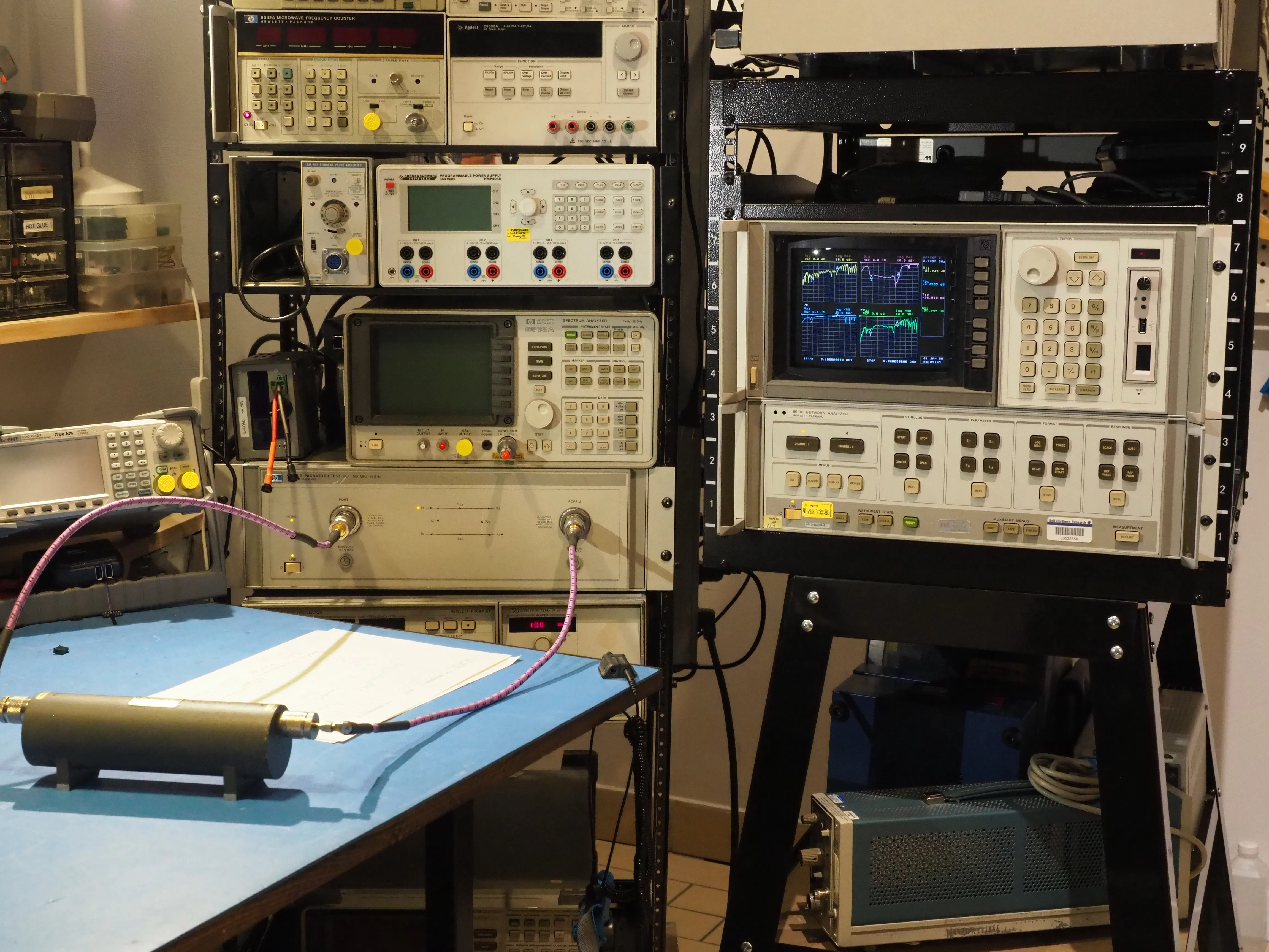
With that in mind, I began collecting parts to assemble an HP 8510C system. As with the HP 8410C, it is comprised of separate units for the display section, IF section, RF source, and test set. Specialized receiver sets are also available for the antenna test system. Most of my units were purchased in untested or broken state, and therefore the total cost was orders of magnitude cheaper compared to a modern platform.
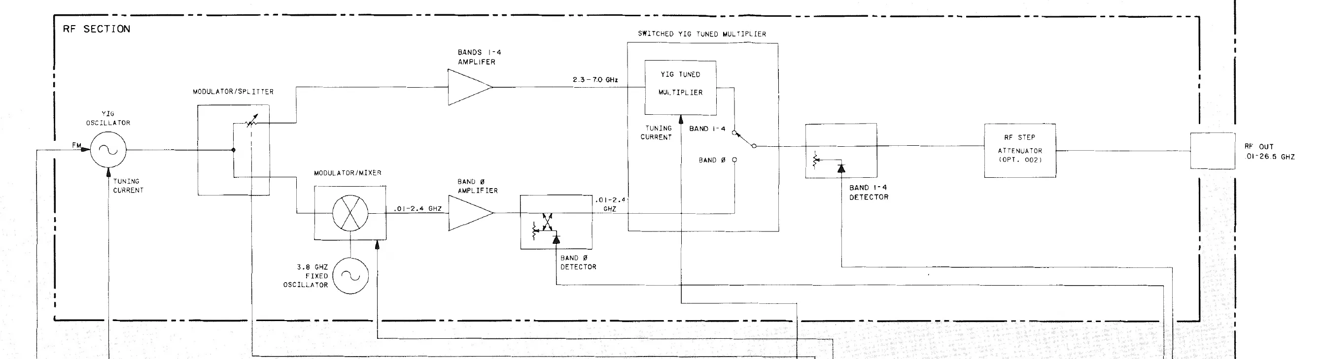
System Overview #
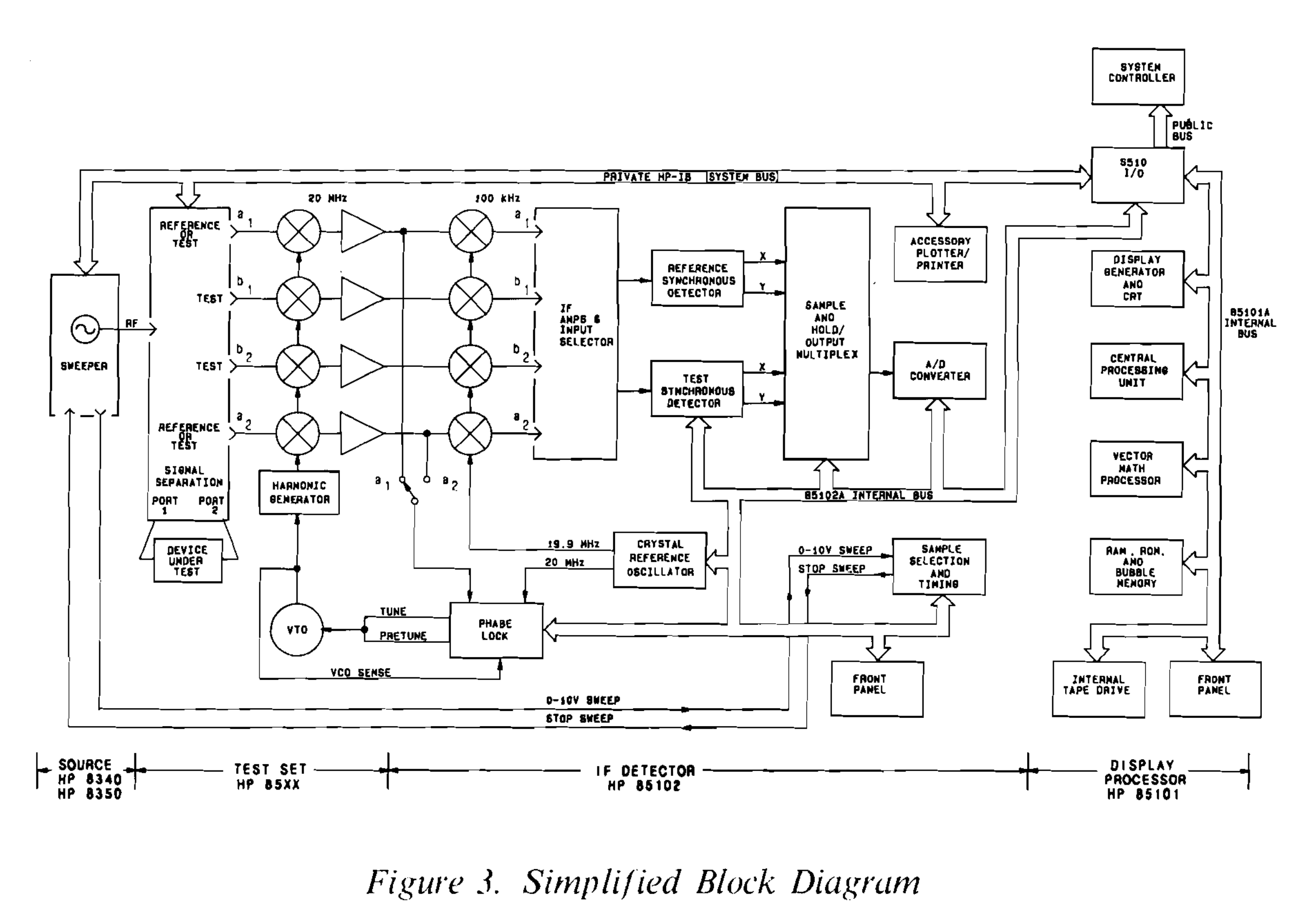
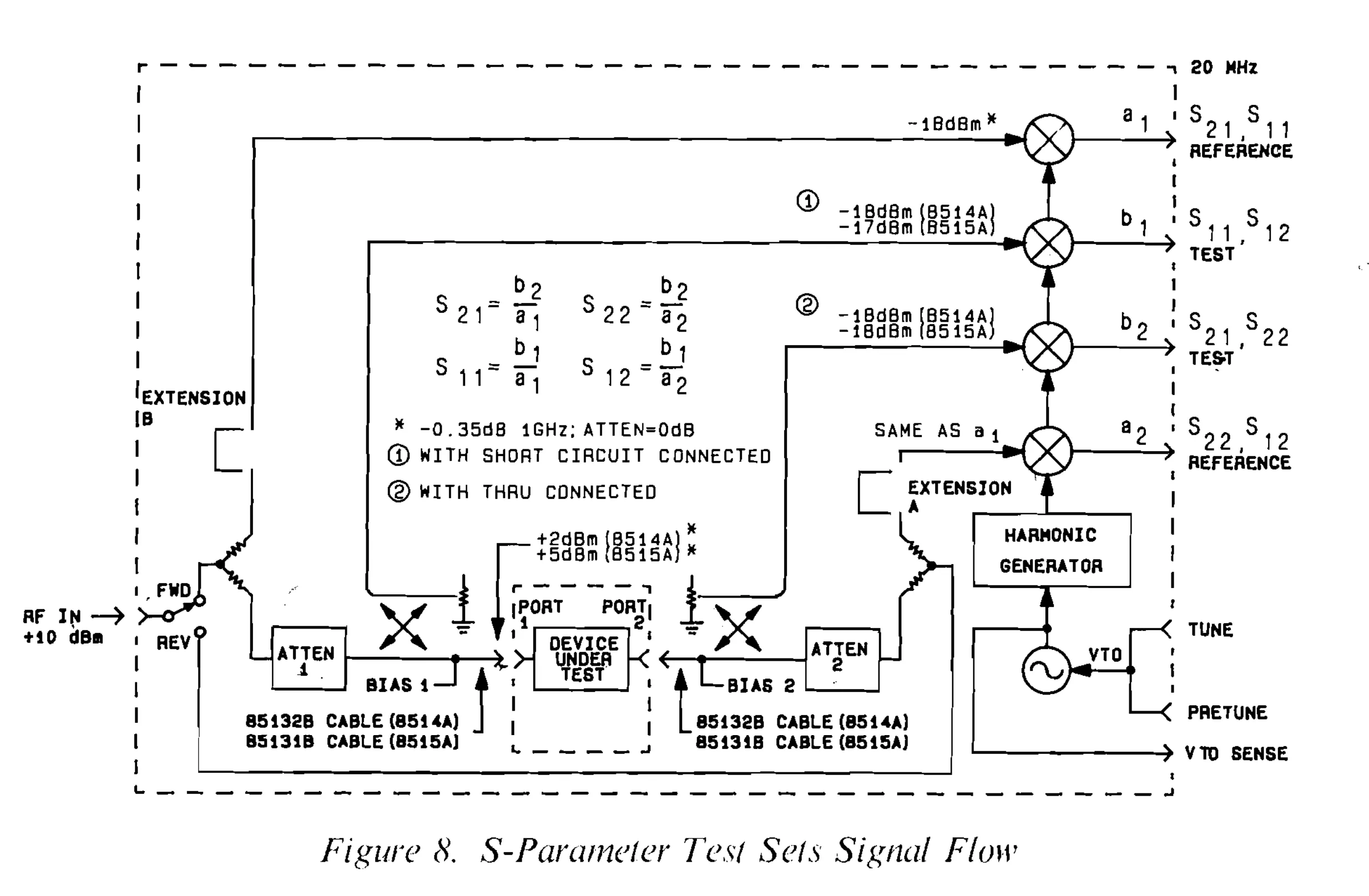
The following block diagram shows the high level flow between source, test set, IF detector, and display. The model below is the “A” suffix. It has a tape drive and a monochrome display. This was upgraded in the “C” suffix to a floppy drive and color display. Dedicated samplers and IF down converters are used for the four reference/test signals. IQ down conversion is performed in the analog domain. A single SAR ADC multiplexes between all channels for digitization.
The sample selection and timing block controls ADC acquisitions in sweep mode, and modulates the stop sweep signal to halt the RF source sweep gen between test set SRD band switches. The internal/private GPIB bus is used for central control of VNA units by the display. The public bus is optionally used for VNA control and data acquisition by an external lab computer.
Display Unit #
The display unit is the digital portion of the instrument. A Motorolla 68K microprocessor coordinates the measurements and UI. The rear has a D-Sub style interconnect to the IF section, internal GPIB bus, public GPIB bus, and RS232 serial. The rear display output appears like a VGA connector, but it uses a special implementation only supported by a few vintage CRT displays.
Display units come configured either as an antenna test set (8530A) or VNA (85101C). Both configurations are physically identical, except for the software and security key. I purchased a 8530A, and converted it to a 85101C.
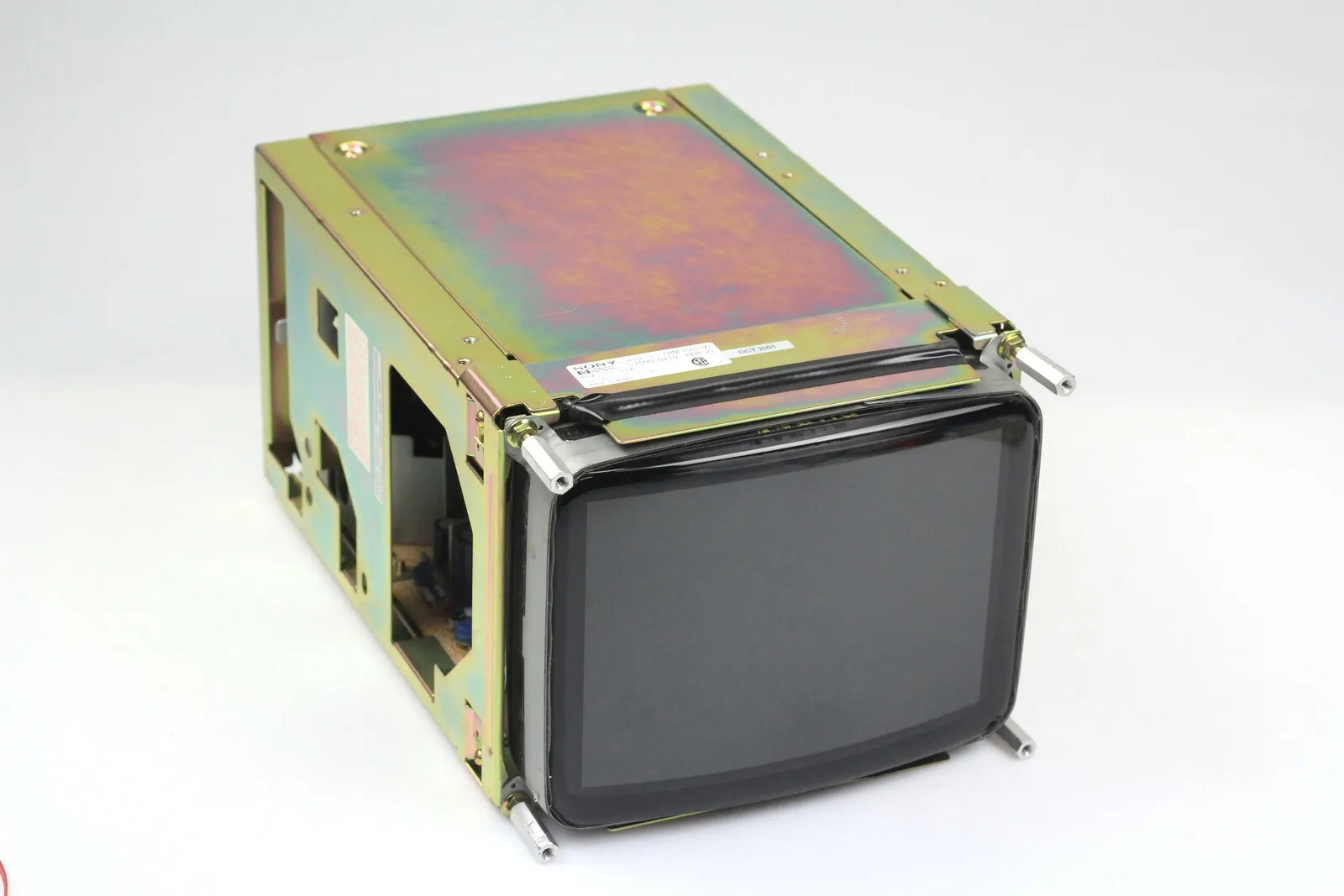
The color CRT in these old HP instruments will go dim and hazy with age. The extent of the fading depends on runtime. Mine was barely legible. It was improved by tweaking the RGB trim pots on the display unit, but far from satisfactory. This could be corrected with a replacement Sony CHM-7501 or an expensive LCD replacement kit from NewScope. In my case, I had a spare CHM-7501 in better condition.
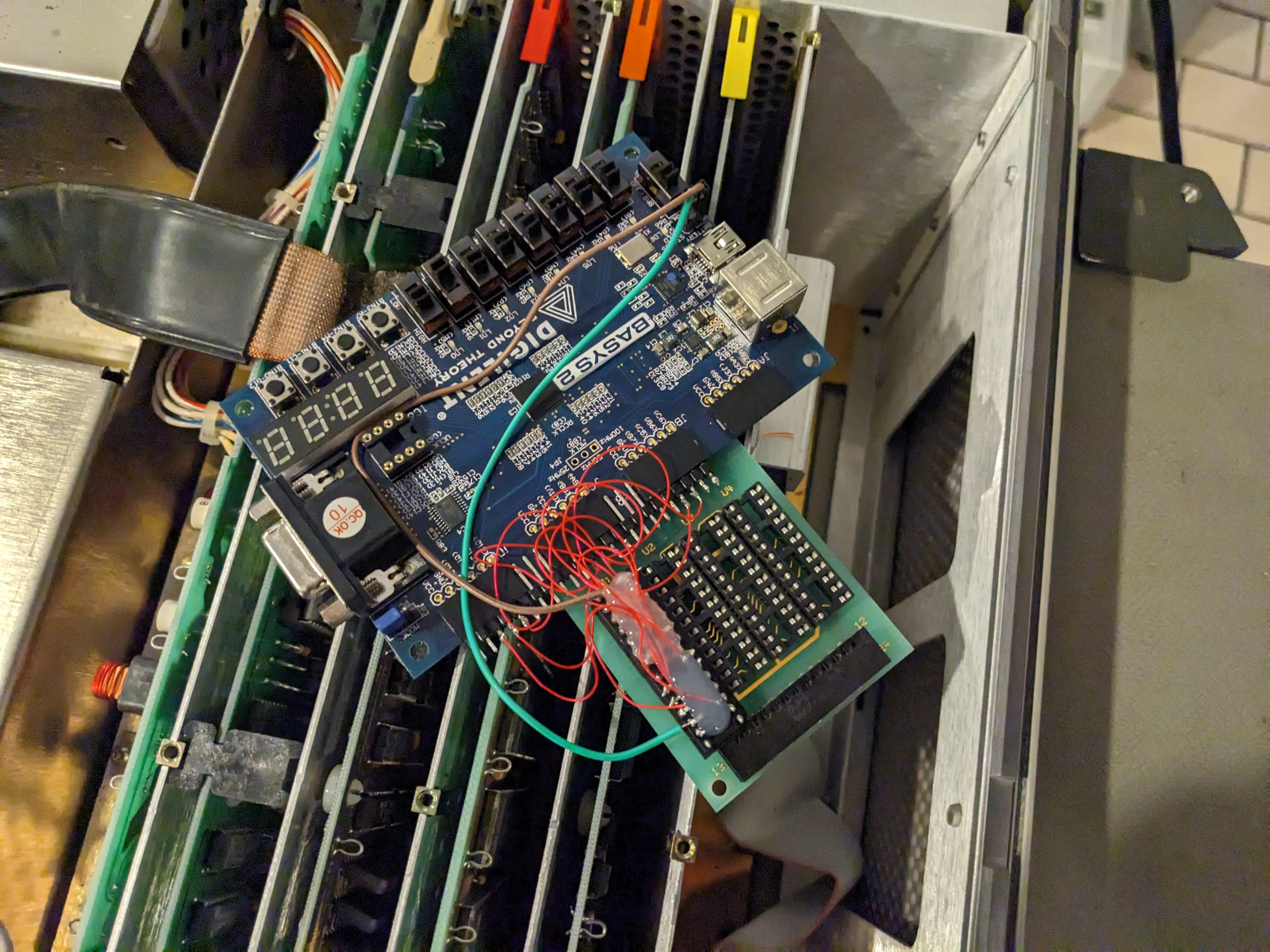
The security key is a removable board with sockets for Programmable Array Logic (PAL) ICs. These PALs are interrogated by the software package on boot to determine if you are licensed for the VNA, antenna test, and/or time domain software. My unit came with the time domain and antenna (8530A) key populated. It would fail to boot into the VNA software. Luckily these PAL keys are trivial to reverse engineer and emulate.
I was able to adapt the above project to an old Spartan 3E FPGA devboard I had laying in a bin. Not wanting to wait for parts, I bodged together a prototype. After installation into the motherboard, I was able to boot into the VNA software without issue. I will eventually print a custom PCB with a low end Efinix FPGA for a cleaner solution. A CPLD would be a better choice, but I did not find any options both cheaper than an Efinix FPGA and with free development tools.
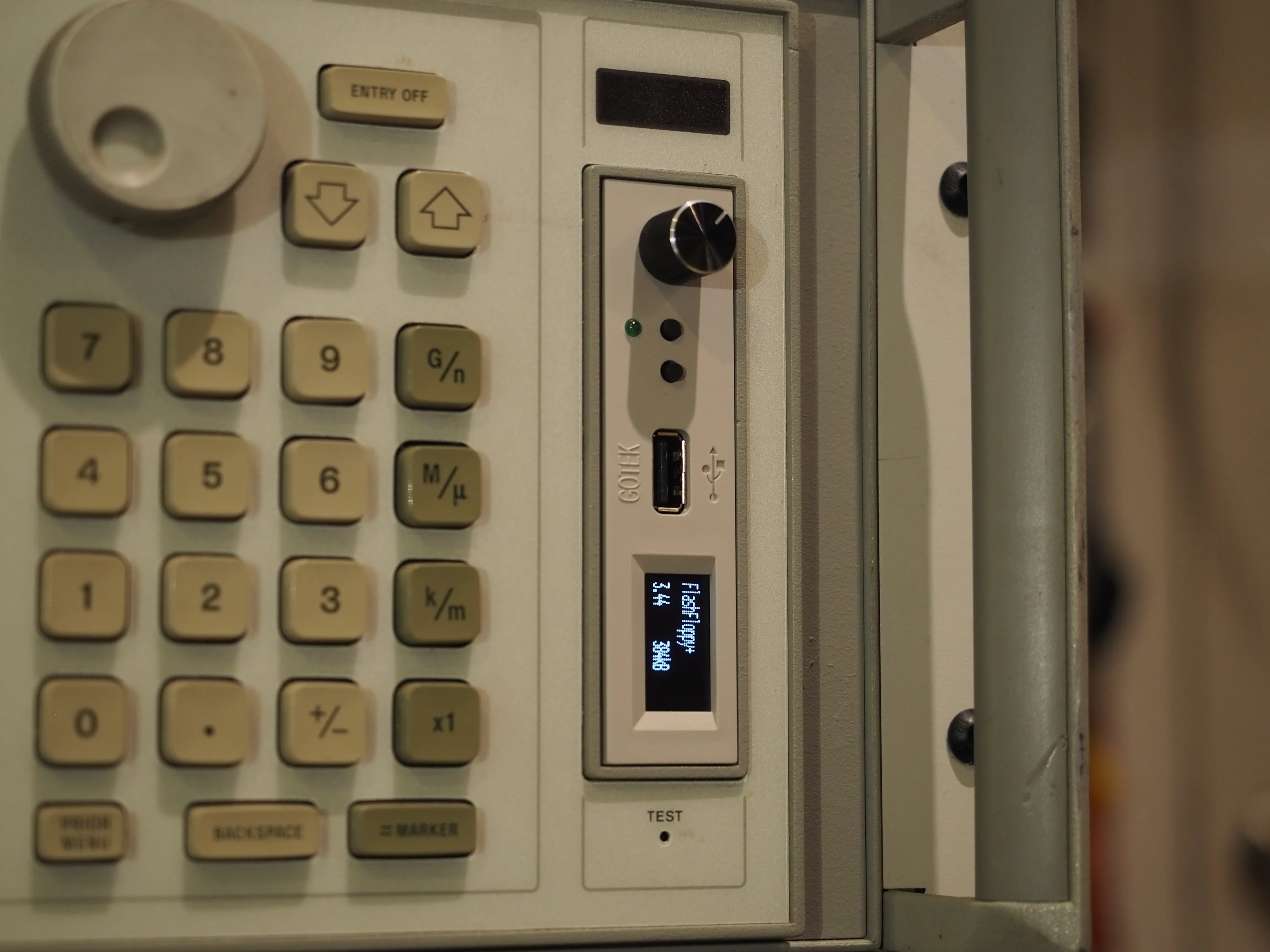
The next hurdle is loading/updating the system software package. By far the easiest option is installing a FlashFloppy to adapt the floppy drive to USB stick. These units can be found cheaply from China. It is highly recommended to buy one explicitly advertising an onboard “AT32F435RGT7” MCU. To install into the HP 85101C display unit, remove the screws surrounding the keyboard, and pull it out. It will then be possible to replace the original floppy drive. The harnesses are pin compatible.
Power on the unit, and update to the latest FlashFloppy+ firmware by following the GitHub instructions. You may then grab the latest system HFE images from the HP8510C FDD Image Repository.
- RF Source
- Test Set
- IF Section
- Display Unit
Specialized Cables #
The 8510C requires specialized interconnect cables:
- Male-Male DB37 Cable. Used for digital interconnect from display to IF section. No twisted pairs or shielding needed.
- GPIB cable from display to test set
- GPIB cable from display to RF source
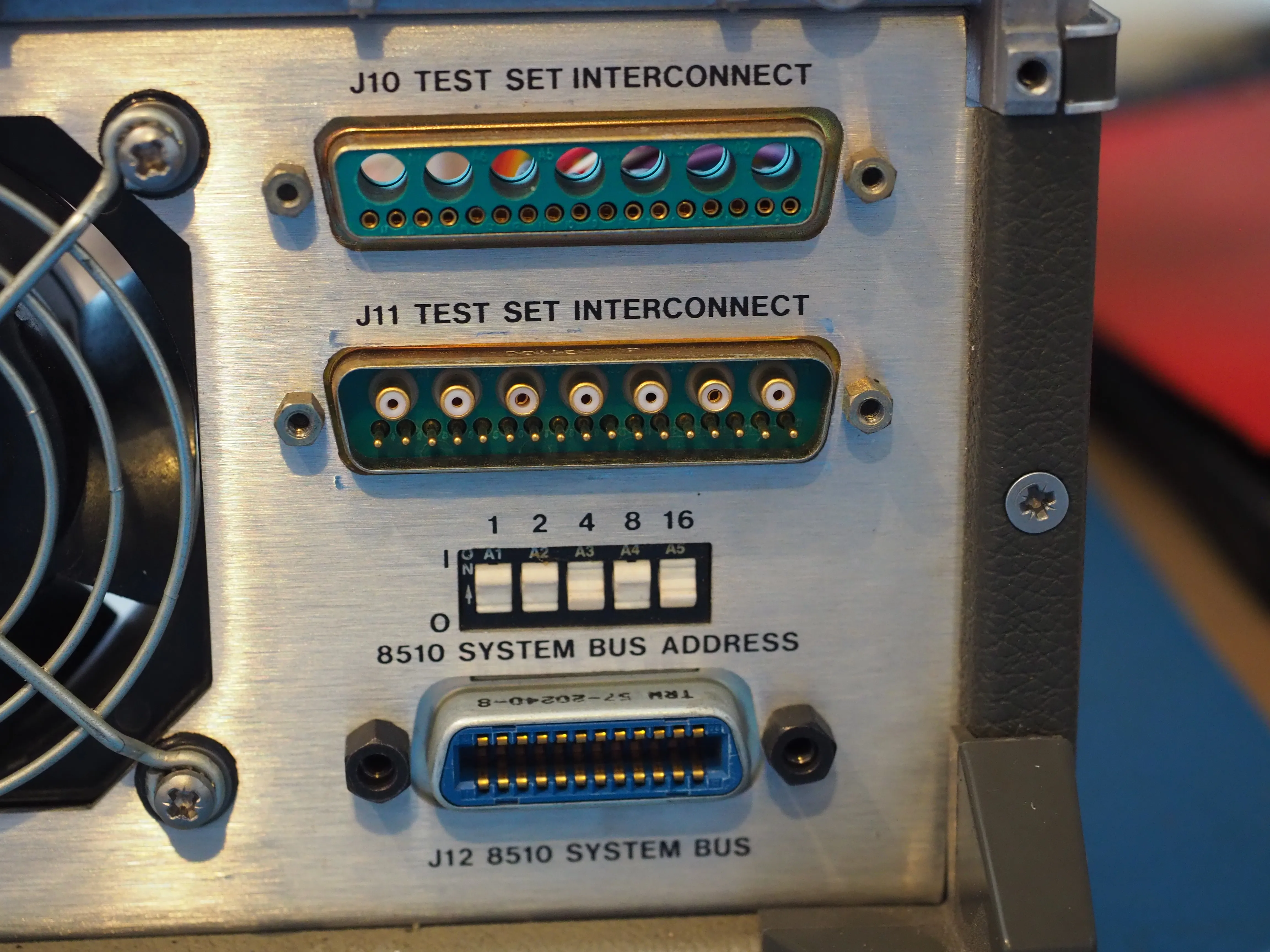
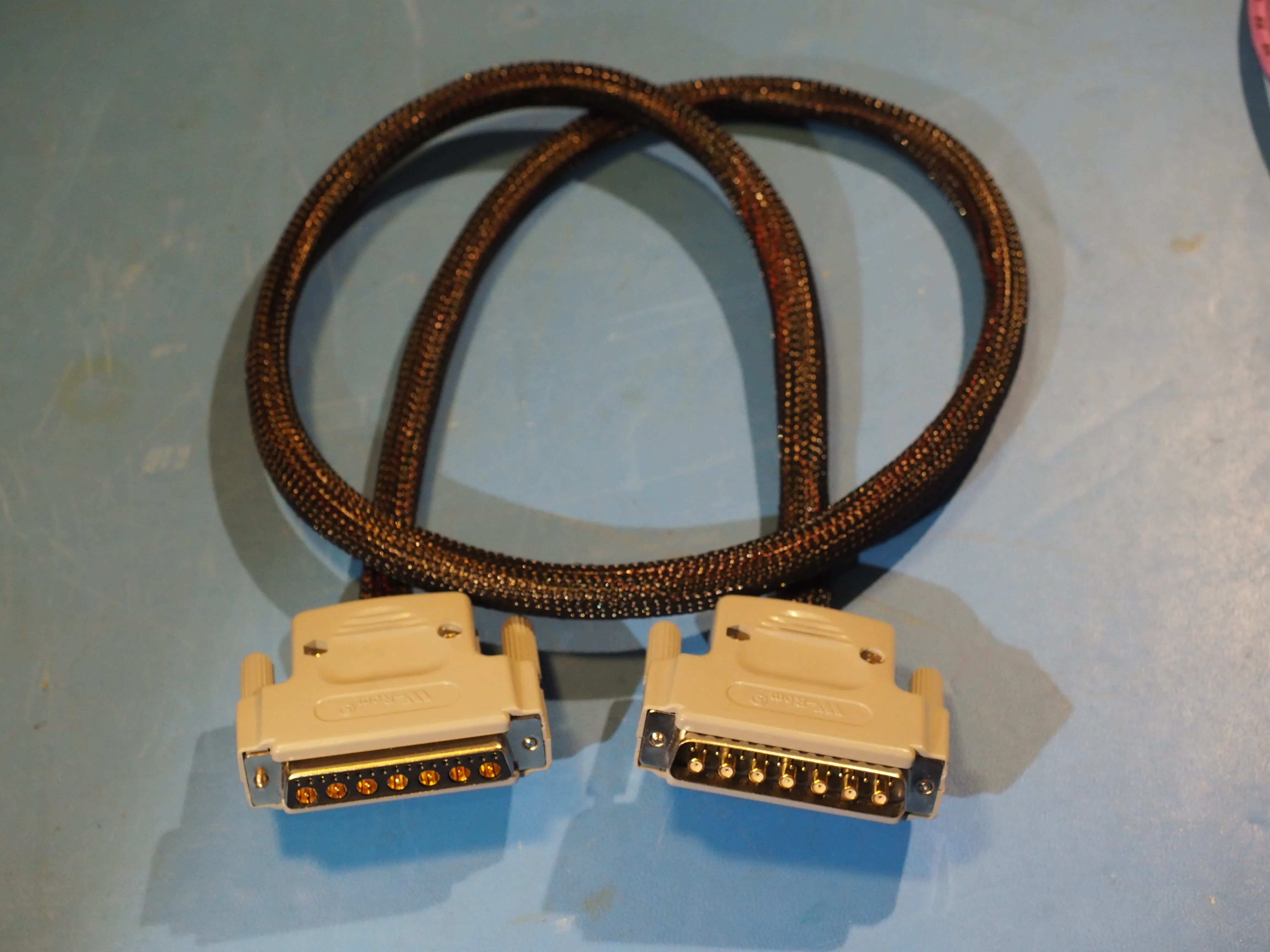
- Male-Female Coax/D-SUB cable from IF to test set (PN: 08510-60102)
- Test set phase extension loop backs (short male-male 3.5mm semi-rigid coax)
- BNCs for sweep control
I used a generic DB37 cable for the display to IF interconnect.
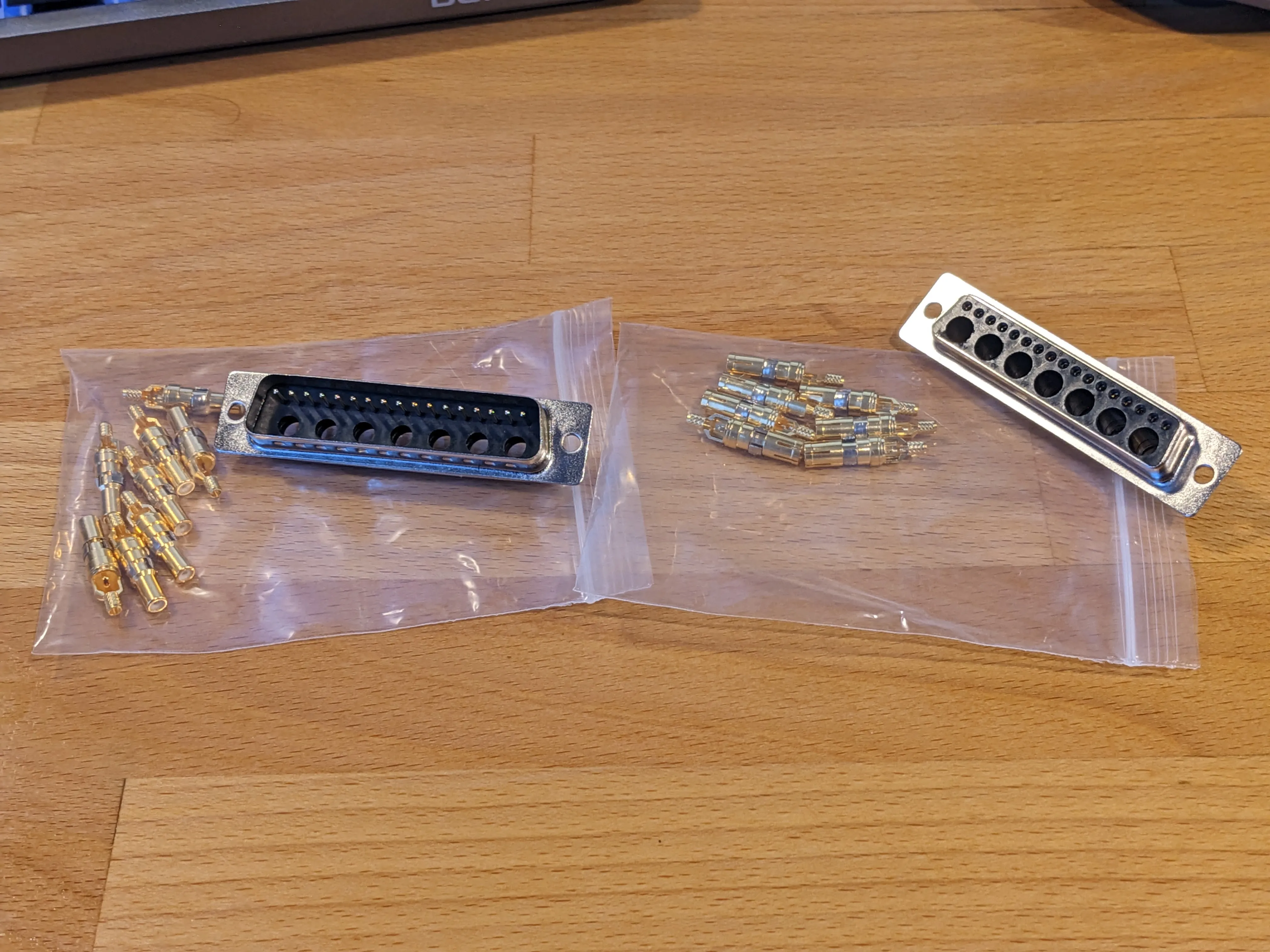
The most expensive cable is the Coax/D-SUB cable from test set to IF. These are mixed DB coax and pin connectors. Cables may be purchased from GLK. I fabricated my own.
Part list:
- RG316 Coax
- Stranded 22AWG copper cable
- DB Male RG316 D-SUB connector (7pcs)
- DB Female RG316 D-SUB connector (7pcs)
- 24W7 Male D-SUB with solder cup connections
- 24W7 Female D-SUB with solder cup connections
- Coax cable crimper
- DB50 plastic housing (2pcs)
- Plastic braided cable sleeve
The 7 pre-installed power pins on the 24W7 connectors can be removed with a metal punch and hammer. Connections are 1-to-1 for both the pins and coax connections. Note the gender differences.
This cable carries the 20MHz IF for the a1, a2, b1, b2 channels. It also carries the tuning voltage for the test set VCO. The test set and IF section form a phaselock system to tune the SRD based samplers to the desired DUT frequency.
IF Section #
The HP 85102 IF section must match the display unit suffix. These are sometimes found field upgraded from a “B” to a “C” suffix. No one has located an HP CLIP for the B/C 8510 units, so upgrading it yourself is probably not feasible.
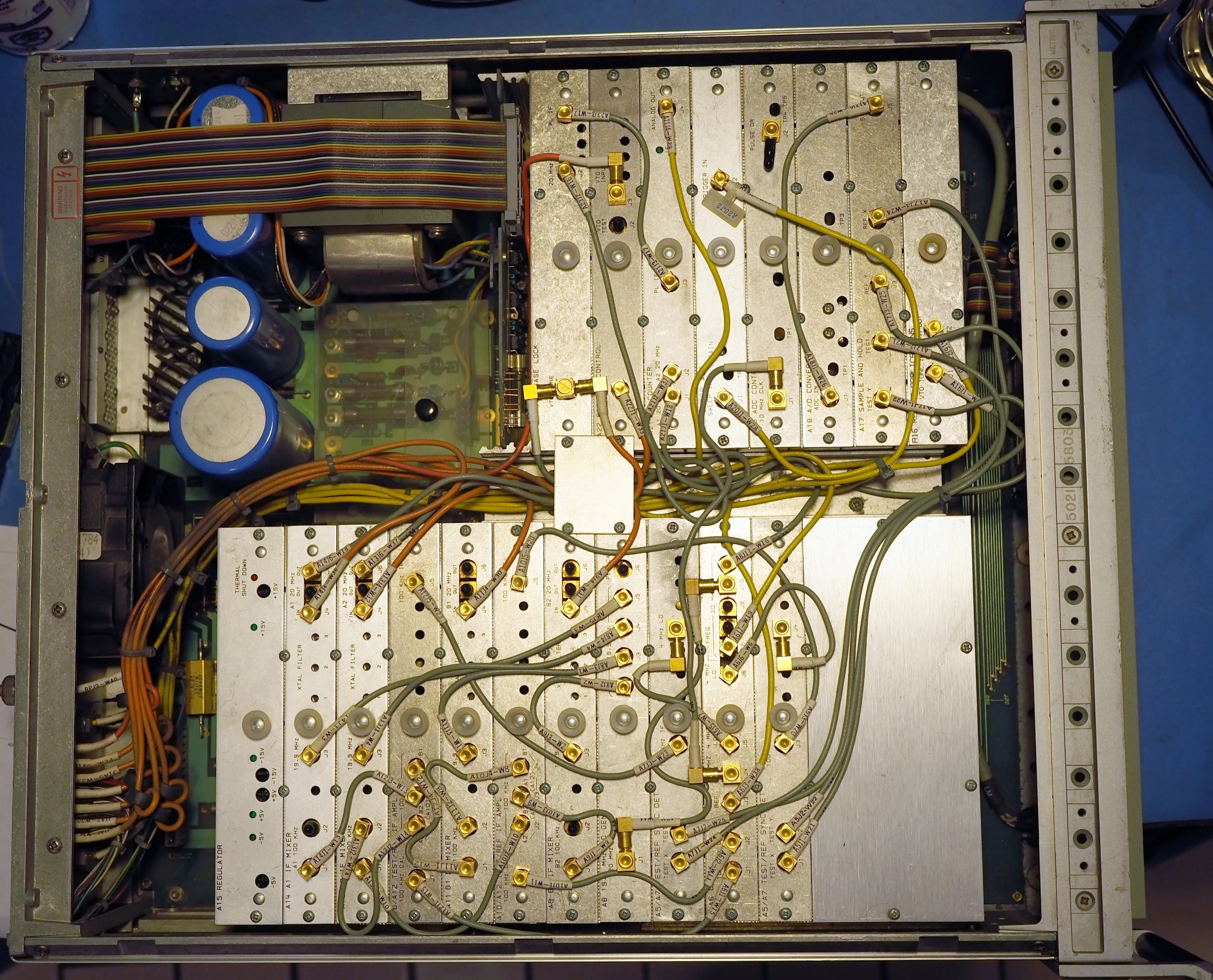
My IF unit was saved from the trash, and in perfect working order. I only needed to remove the front key panel to free up the button mechanisms with silicon lube.
Test Set #
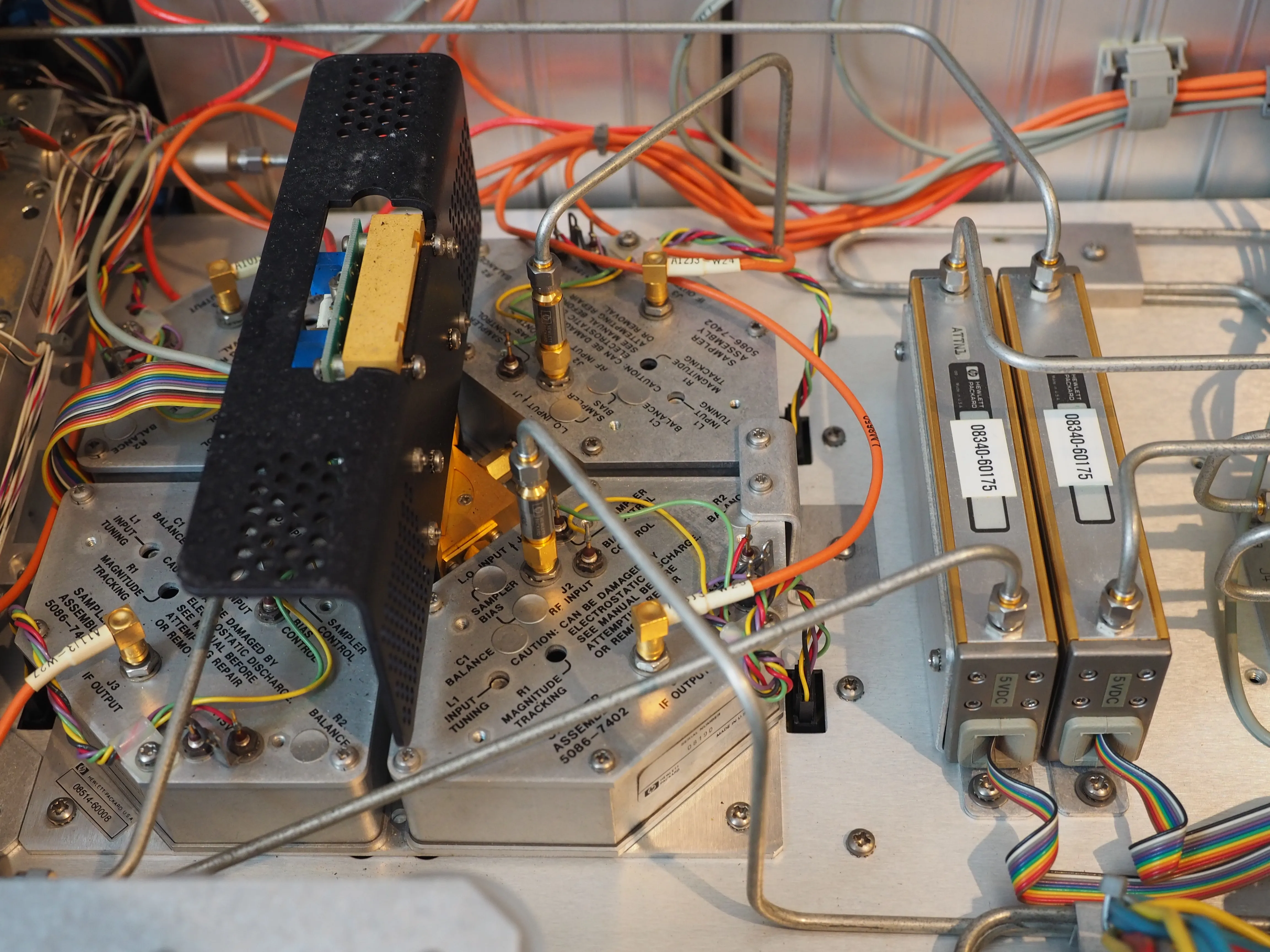
The HP 8514A S-Parameter test set is rated from 500MHz to 18GHz. It can operate down to 45MHz if loss of dynamic range (-30dB) is acceptable to your application. It includes inline 90dB step attenuators for each channel, allowing a wide range of incident power on the DUT. This is useful for amplifiers, and compression testing. Other test sets are available for wider frequency spans if needed. Mine was functional after replacing a blown fuse, and fabricating the missing phase extension loop back cables.
RF Source #
Several RF source options are supported. The HP 8510C Preflight Checkout document is handy to ensure all the firmware variants and interconnect requirements are satisfied.
The HP 8340A/B and HP 8360 series sources are the most desirable options. They are synthesized sources, and result in faster sweep times. They remain extremely expensive on the used market.
The HP 8350B mainframe is the cheapest option. I already owned an HP 83592B (10MHz to 20GHz) source unit, and mainframe.
My source unit was initially exhibiting low power (ALC unlevel). This was repaired by a full reassembly, re-torquing the SMA connectors. The unit is a tight packed maze of rigid line coax and RF modules. It’s a marvel of mechanical packaging, and a servicing nightmare. After reassembly, I could adjust the YTM “peak” knob on the front panel to achieve the rated power output at fixed frequency points. Sweeps would still fail with ALC unleveling.
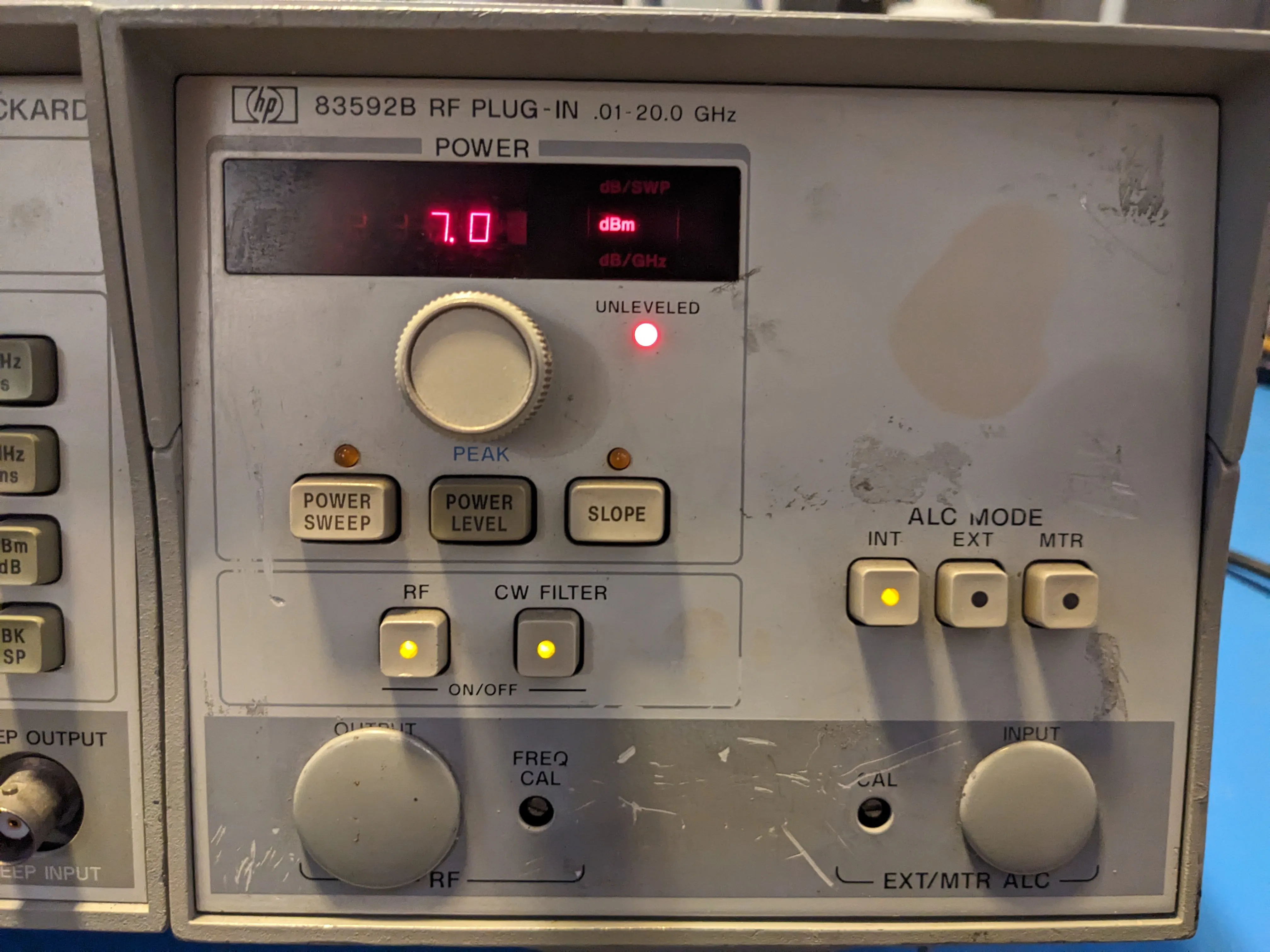
Those symptoms strongly indicate the YIG filter in the YTM is not being correctly tuned in sweeps.
The service manual provides a procedure to adjust the internal DIP switches to set the YIG filter driver gain and offset for each of the frequency bands. Since I did not have a scalar network analyzer for this adjustment, I used a crystal detector and oscilloscope in X-Y mode. This was sufficient as I only needed relative power measurements to peak the response across each band. Performing this adjustment fully repaired the unit across the full sweep range.
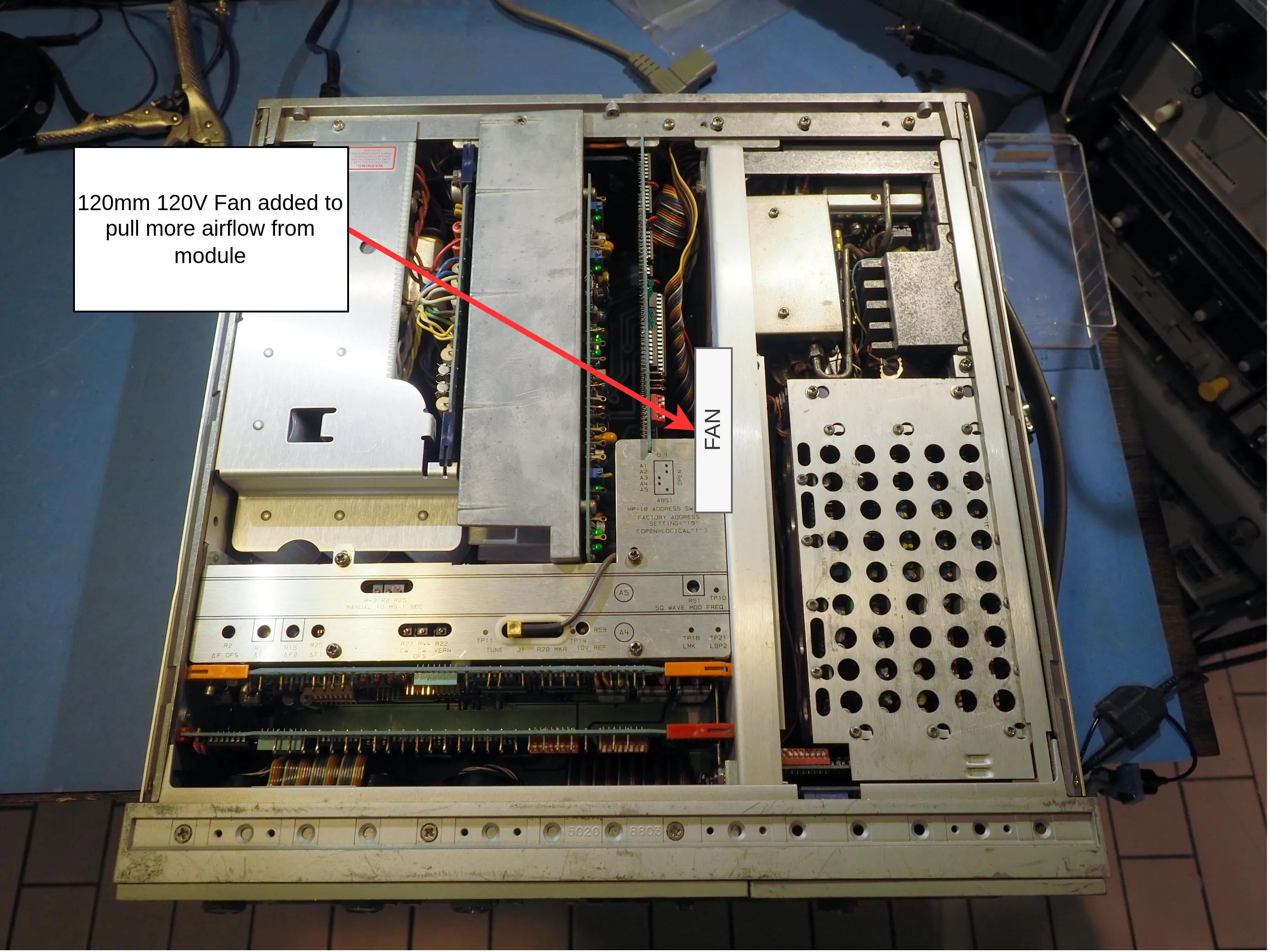
These HP 8359x plugin modules are densely packed, and the YTMs can fail due to prolonged overheating. If you have a good unit, I strongly suggest you add an additional fan in the frame to keep the unit cool. The YTMs are unrepairable without a deep access wire bonder.
My 8350B mainframe also required some minor repair. The front encoders were nonfunctional. These early HP RPGs have a fixed lifetime. They use a tiny T-1 incandescent lamp as the optical encoder light source. Mine were burnt out, but easily replaced with a model from DigiKey:
| PN | Description |
|---|---|
| VCC7216-ND | LAMP INCAND T-1 WIRE TERM 5V |
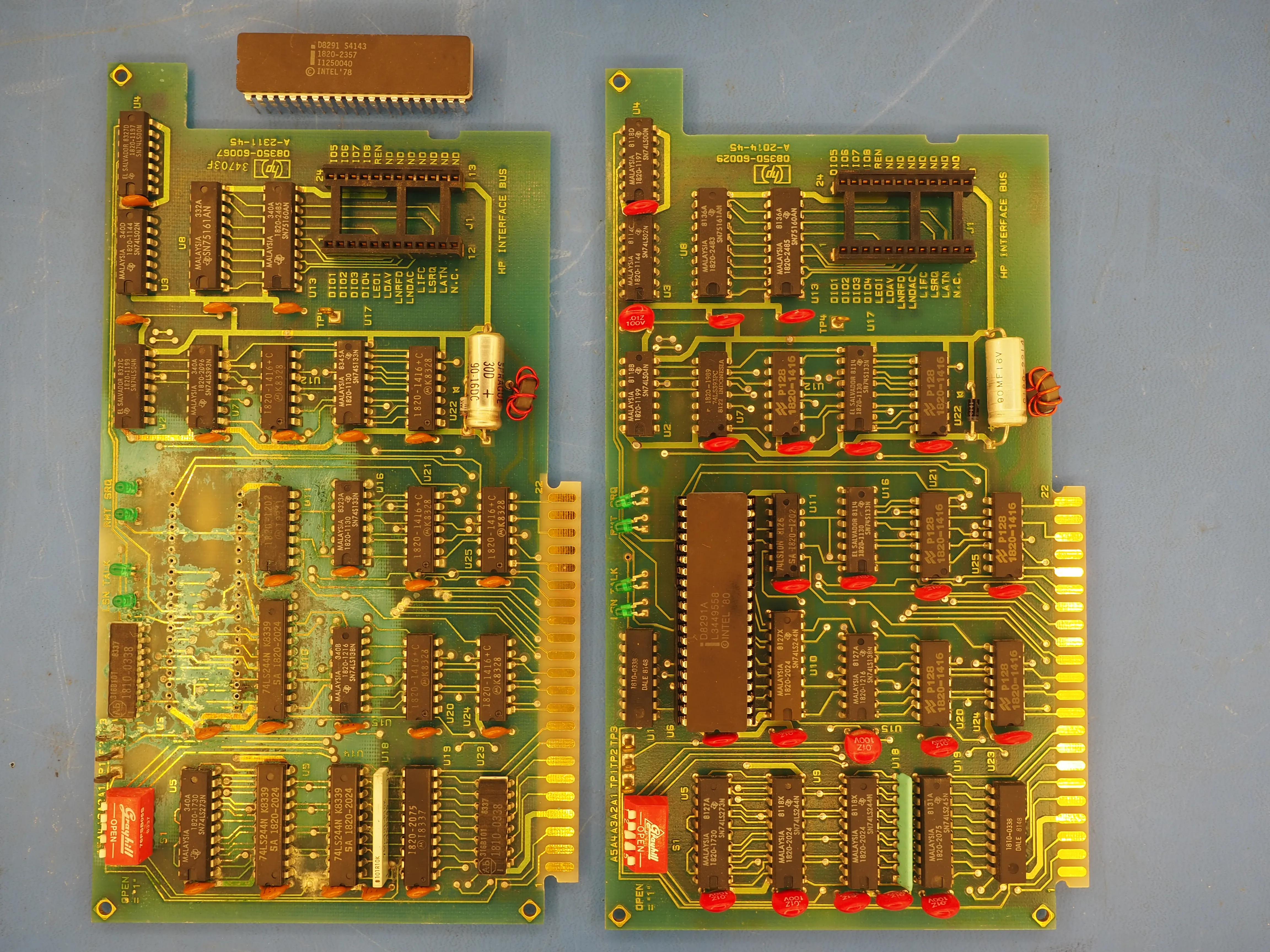
The NiCD battery pack also leaked out onto the GPIB PCB, ruining most of the traces. I tried repairing the traces with mod wire, but the damage was too severe. I swapped it out with a spare GPIB board from my older HP 8350A.
Troubleshooting #
After all of that effort, I assembled my system and found it only would capture in single frequency points. A sweep measurement would fail with a red asterisk. Start/stop frequency could not be adjusted. Frustratingly, no error code was presented. After probing the sweep control board on the IF section with a logic analyzer, I narrowed the issue down to a hang on the system GPIB bus.
The GPIB bus was hanging because of my foolish swap of GPIB PCB from an HP 8350A sweeper. Even though I previously verified the schematics were identical, I missed a critical BOM change. In the “B” variant, HP changed the main GPIB controller IC from a D8291 to a D8291A. The A suffix indicates a later IC revision with additional GPIB extensions. Luckily the D8291A on my NiCD acid eaten board was still functional, and swapping ICs brought this VNA to life.
Plotting #
The 8510C supports most of the HP pen plotter lineup. Just set it to the correct GPIB address, connect to the instrument bus, and click the copy button. Plotter emulator software with a GPIB-USB adapter is another option for digital copies.
Calibration #
Calibration on this instrument is highly configurable. Cal kits can be defined manually with the keypad, but a USB-GPIB adapter dramatically simplifies the process.
The 8510C can store coefficients for up to 2 cal kit models. There is no preset option for a generic SOLT cal. The default cal kit definitions are for an HP 3.5mm and 7mm kit, which require a sliding load to complete a cal sequence. Purchasing a professional mechanical cal kit from Keysight would cost 10x what I paid for my entire VNA system, so a DIY approach is needed.
The coefficients are uploaded via GPIB with a windows program from HP: VNA Cal Kit Manager V2.1. You may also use this program to create your own custom cal kits.
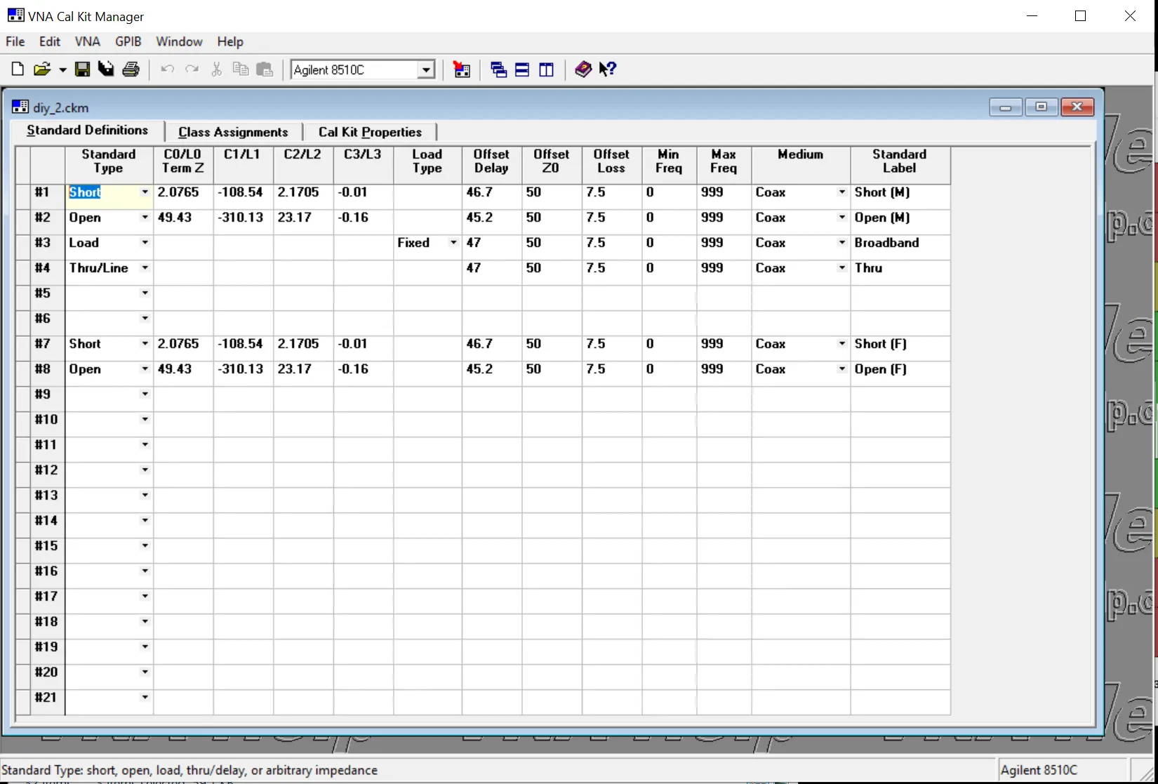
The cal kit coefficients use a standard HP format modeling various circuit elements (offset delay, loss, capacitance, inductance). Capacitance and inductance are expressed as frequency dependent polynomials. If accuracy is non critical, you may create “ideal” cal kit coefficients for an SOLT style coaxial calibration.
I used a Keysight PNA + ECal to measure the response of my own 3.5mm SOLT kit. This is needed to create custom models, and to confirm their corrected performance is sufficient for accurate measurements.
I purchased a handful of high quality 50 Ohm termination and thru rated to 27GHz. I then chose the termination with the lowest return loss, and thru with minimum insertion loss. Load+thru return loss is your limiting factor, and should be as low as possible. Mine measured a respectable -38dB at 10GHz.
I wrote a Python script to curve fit the HP model coefficients from my SOLT kit based on my measured responses. Some hand tweaking was still required. The scikit-rf page on SOLT Calibration Standards Creation is a useful resource to learn about how these standards are modeled.
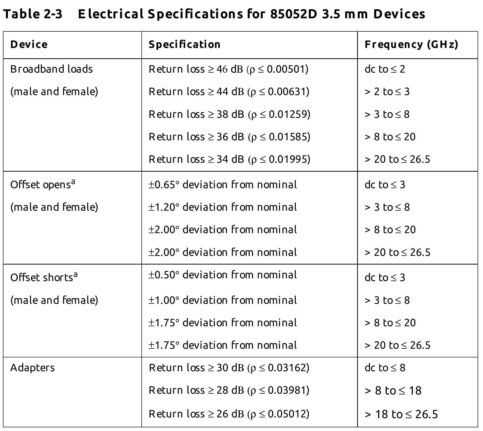
My short and opens were from an inexpensive kit. After deembeding my offset delay model, I confirmed their phase difference remains at 180 deg with only a +- 2deg deviation across their frequency range. It is critical to accurately model the “Offset Delay”, otherwise the measurement phase error will be excessive. For comparison, see the following table for a 26.5GHz cal kit from Keysight.
The HP 8510C C/L models are third order polynomials, and thus can’t correct for all responses. I found that even after careful tuning of my coefficients for the HP 8510C, I got higher accuracy results using scikit-rf SOLT calibration on an external PC. The algorithm in scikit-rf directly uses measured touchstone responses of your SOLT “ideals”, and is not limited to the third order curve fit.
Scikit-rf Virtual Instrument and SOLT #
Scikit-rf has a handy module allowing for direct captures from your HP 8510C over GPIB. The output is packaged as a scikit-rf network. Many tools are then available for calibration, deembeding, concatination, and plotting.
Example of a 2-port measurement using a GPIB-USB adapter:
import skrf

vna = skrf.vi.vna.hp.HP8510C(address='GPIB::15::INSTR', backend='@py')
vna.set_frequency_sweep(500e6,18e9,801)

meas_ntwk = vna.get_snp_network(ports=(1,2)) # Measure 2-Port Network
Example of scikit-rf SOLT calibration:
# Ideals
ideal_short = skrf.Network('short.s2p')
ideal_short = skrf.subnetwork(ideal_short, [0]) # Trim to a 1-port network
ideal_shorts = skrf.two_port_reflect(ideal_short, ideal_short)

ideal_open = skrf.Network('open.s2p')
ideal_open = skrf.subnetwork(ideal_open, [0]) # Trim to a 1-port network
ideal_opens = skrf.two_port_reflect(ideal_open, ideal_open)

ideal_load = skrf.Network('load1.s2p')
ideal_load = skrf.subnetwork(ideal_load, [0]) # Trim to a 1-port network
ideal_loads = skrf.two_port_reflect(ideal_load, ideal_load)

ideal_thru = skrf.Network('thru.s2p')

ideals = [
	ideal_shorts,
	ideal_opens,
	ideal_loads,
	ideal_thru,
]

measured = [
	skrf.two_port_reflect(s11_meas_short, s22_meas_short),
	skrf.two_port_reflect(s11_meas_open, s22_meas_open),
	skrf.two_port_reflect(s11_meas_load, s22_meas_load),
	s21_meas_thru,
]

cal = skrf.SOLT(
	ideals = ideals,
	measured = measured,
)

cal.run()
cal.name = "solt test 1"
cal.write()
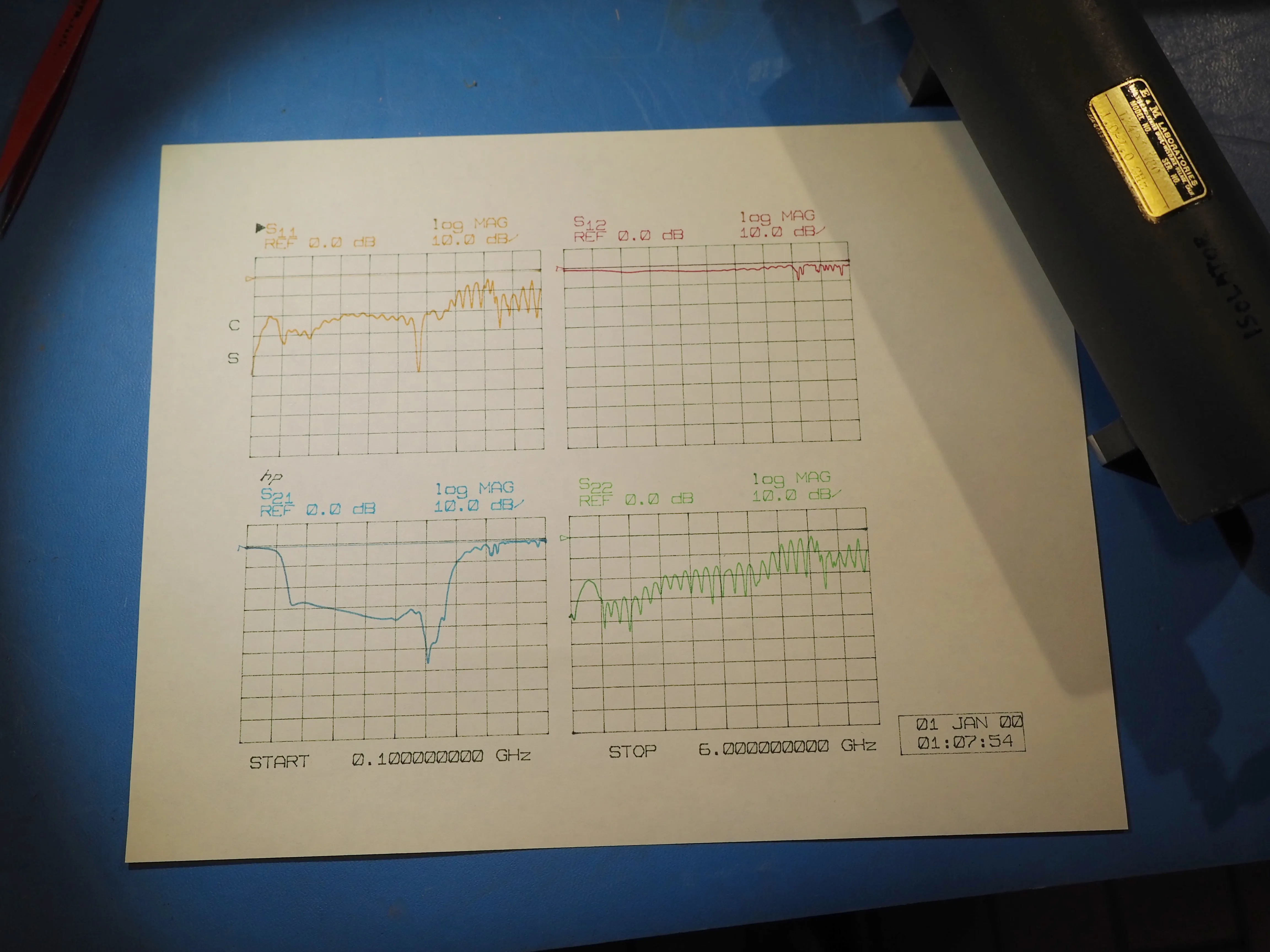
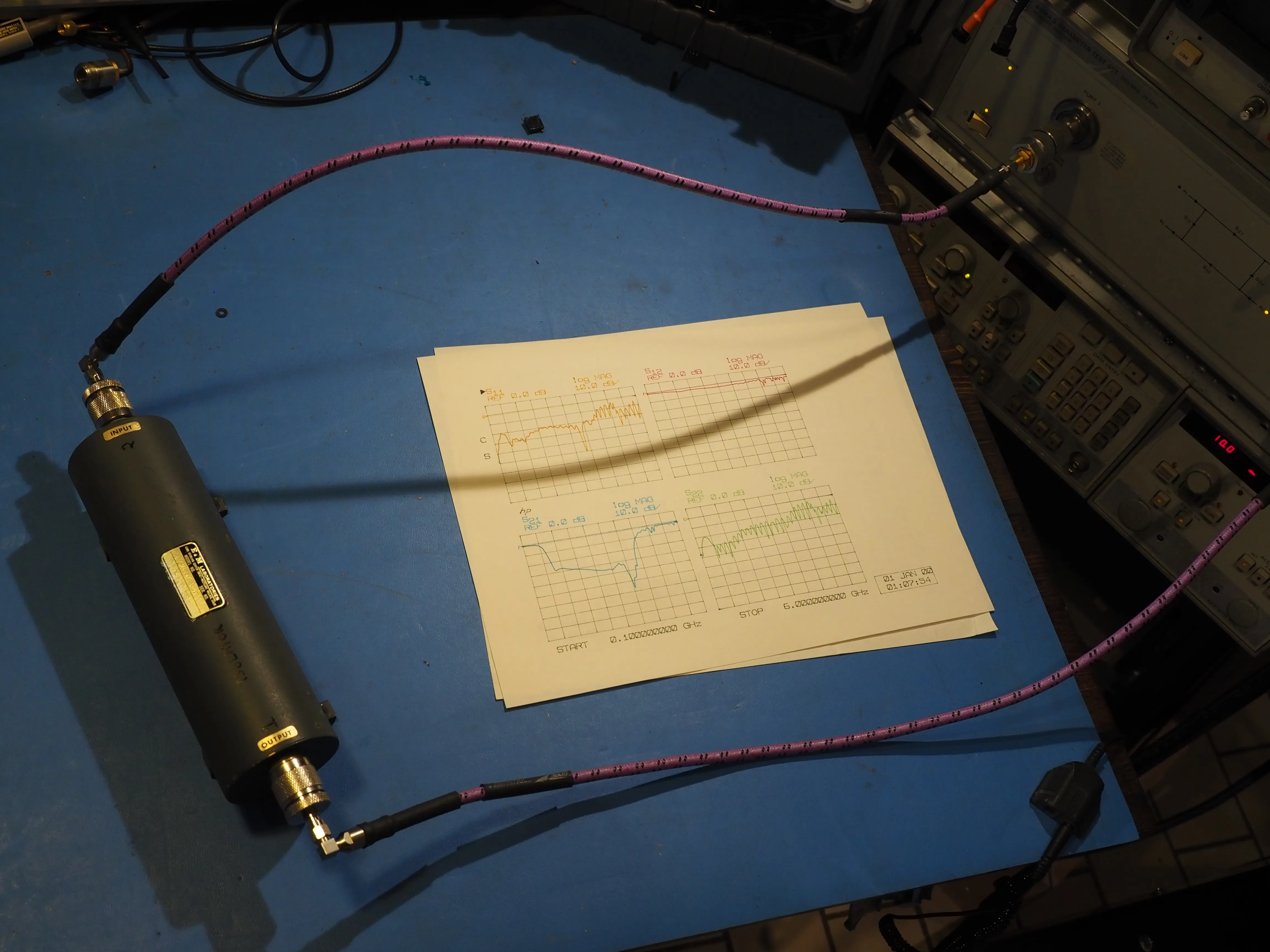
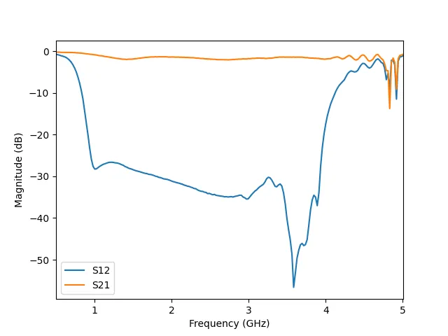
Measurement of a 1-2GHz RF Isolator. SOLT calibration applied in scikit-rf.
Calibration Accuracy T-Check #
Verifying the accuracy of a VNA calibration is typically performed with a precision stepped impedance air lines, or a t-check. Keysight sells stepped air lines for this purpose, but they retail for over $14k. A t-check is more attractive as it can be built with less precision. It is constructed as a T junction, with one port terminated to a restive load. Accuracy depends only on the assumption that the T junction is lossless. The exact value of the termination load is non critical.
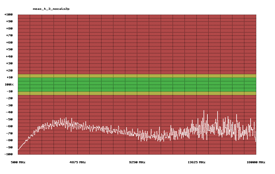
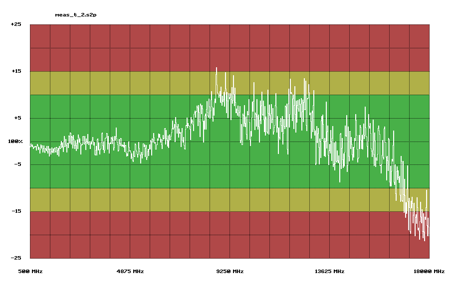
Below is a DIY t-check made from two vertical launch SMA connectors, a 100 Ohm SMD resistor, and some copper foil. The foil was fully wrapped around the center conductor with an air gap of ~2mm. All gaps between the foil and connectors were soldered shut. This construction is crude, and only intended for a rough confidence check at lower frequency.
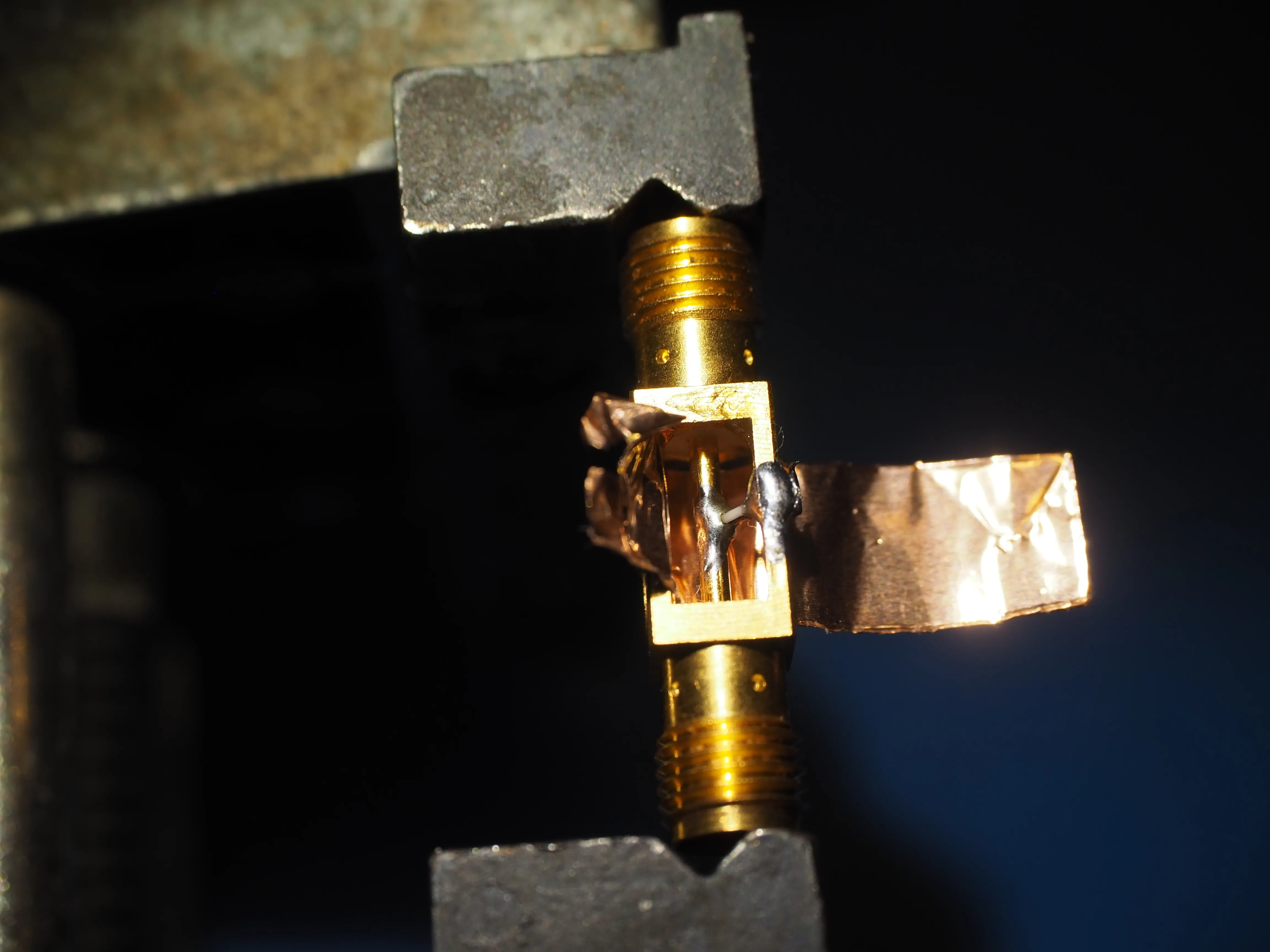
The KE5FX GPIB Toolkit has a standalone utility which can be used to perform a t-check of any S2P file. Below are results before and after calibration. The results are much better than expected given the rough construction. It would be interesting to take this measurement on a professionally calibrated VNA to compare results.
Rack mounting #
One thing to consider with this system is mounting it in your lab. The rear IO must be accessible, so the only good option is rack mounting. The test set must be close to your table to minimize cable length to your DUT. The test set should also be close to the RF source, so you can interconnect them with a minimal length of coax. I used my main 34U rack for the test set and RF source, and a secondary 9U rack on a tool stand for the display and IF section. This was a great solution for me. Note that you will need rails to support this type of gear. I used some 2.5mm thick shelving angle bar for this purpose. Assembling an HP 8510C system can be cost effective, but it will never be compact.